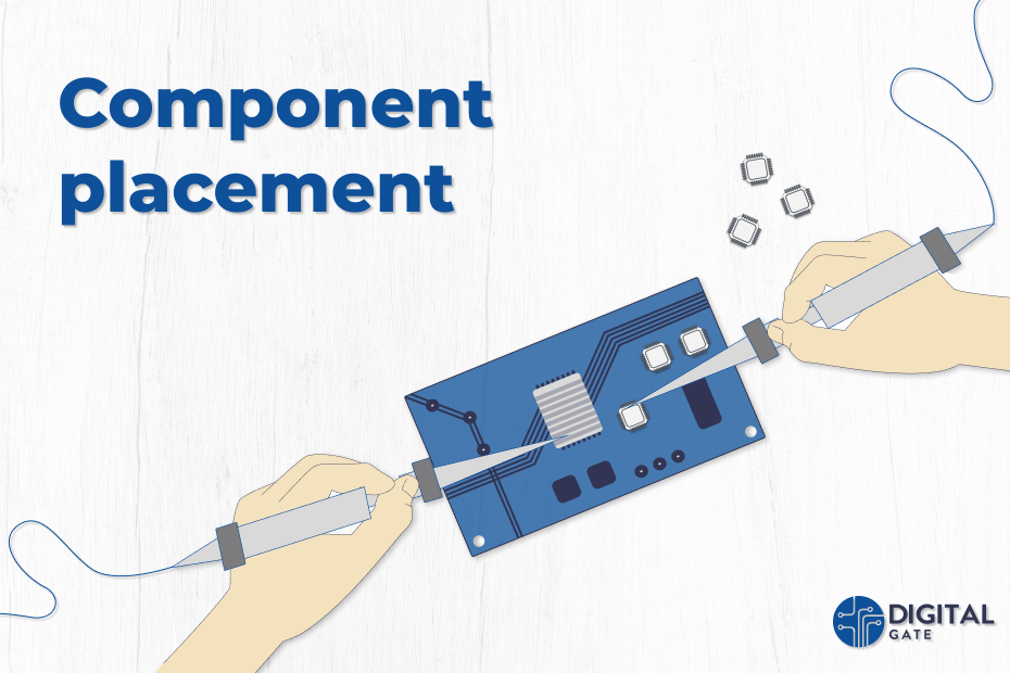


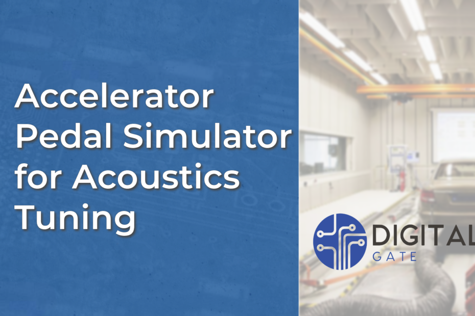
Accelerator Pedal Simulator for Acoustics Tuning
Have you ever wondered how the perfect roar of an engine, or the smooth hum of a luxury car is crafted? It all comes
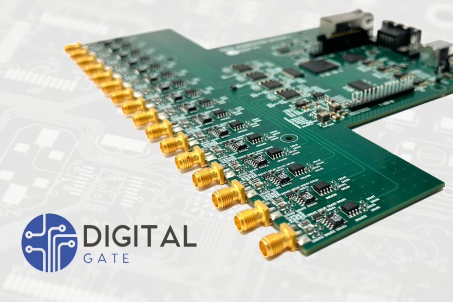
Industrial Data Acquisition System
We’re excited to unveil one of our flagship products: an efficient and secure Data Acquisition System (DAS). Our team has designed this solution to
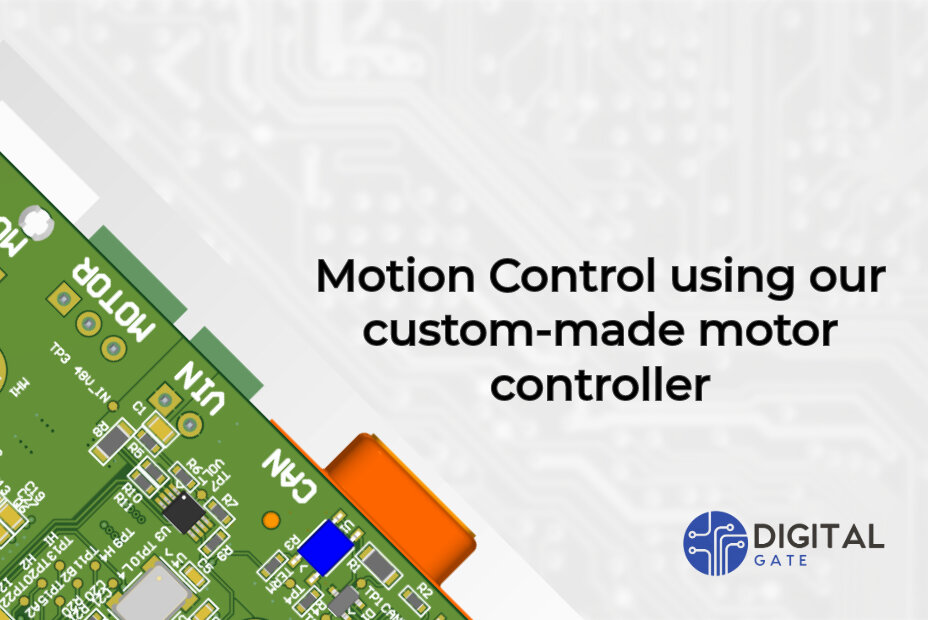
Optimizing our Custom Motor Controller for Motion Control
Using our carefully designed board, we demonstrate the impressive power and flexibility of integrating modern technologies into motor controllers. In the realm of small
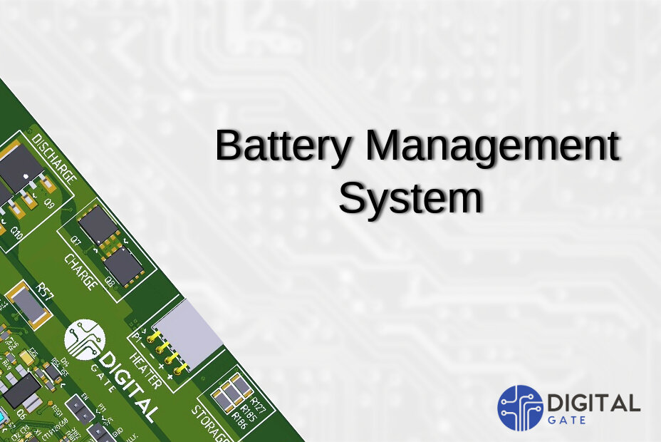
What it means to make an efficient Battery Management System?
Digital Gate is excited to introduce you to one of our flagship products: an efficient and secure Battery Management System (BMS), meticulously designed and

Embedded World 2024
DigitalGate is excited to announce its forthcoming participation at Embedded World 2024 taking place in Nuremberg from the 9th to the 11th of April.
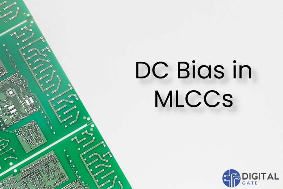
Capacitance Preservation: Strategies for DC Bias in MLCCs
Is the capacitance of the capacitor always same? Multilayer ceramic capacitors (MLCCs) offer several advantages that make them a popular choice for various electronic