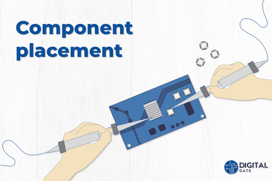
Component placement is one of the most critical parts of PCB design. First, you must understand the fundamental criteria for arranging components on a printed circuit board. Then, you should understand how they impact other areas of your design process (MCAD enclosures, production, signal integrity).
Improper component placement can cause a slew of problems that compromise the PCB’s functionality, longevity, manufacturability, and serviceability. A certain way to compromise the analog signal is by placing analog and digital components together without sufficient segmentation.
Signal integrity (crosstalk, reflections, attenuations, ringing) and electromagnetic interference are the most common problems we encounter when designing high speed PCBs.
This is how a PCB design process looks like:
- Schema Creation;
- PCB File Creation ;
- Creating a board shape;
- Design Rules;
- Stackup development;
- Placement of components; <– We are here
- Routing;
- DRC check;
- Preparation of documentation;
- Generating Files for production.
- Circuit block: To begin, arrange components that collaborate to do certain tasks in the system. All components involved in power regulation, for example, should be grouped together.
- Large Processors: These components contain a lot of I/O and will connect with your grouped circuit blocks directly. Arrange the first-level circuit blocks around your central processor, then the downstream circuit blocks around them.
- Access to routing channels: Attempt to arrange them so that their pins are facing each other if you have a group of components that all need to access the same interface on another component, This won’t always be feasible, but if it is, you won’t have to route via internal layers or around other components in long journeys.
Preparing for Layout
A good method to start you high-speed PCB layout is to create a floor plan for your project. By planning ahead, you can account for groupings of components, such as those indicated above.
Heat Management
The voltage regulator warms up dramatically in high-power situations. You’ve likely incorporated some heat dissipating vias to boost the heat dissipation rate. You should not place other components near the regulator, though. The same rules apply when employing a power op-amp or another heat-emitting device.
135 ⁰ trace bends instead of 90 ⁰

Try to maintain the number of bends to a minimum when routing high-speed signals. You should use 135° bends, instead of 90° bends. At 90 degrees, smooth PCB etching is not guaranteed. In addition, very fast sharp edges operate as an antenna.
The length of the connection

Also, make connection lengths as minimal as possible while planning your placement. Additionally, try to arrange the components in high-speed signal routes (multiple nets that connect a sequence of components together) as near together as feasible rather than spaced out. Be sure to account for your routing channels to ensure that you have enough room when arranging your location.
Do not place any components or vias between differential pairs!

You should maintain consistent spacing between high-speed differential pairs, while routing them parallel to each other. This distance aids in the attainment of the desired differential impedance. The region where the prescribed spacing is expanded due to pad entries should be minimized by the designer. You should route the differential pairs symmetrically.
Try not to place components or vias between differential pairs. Components and vias placed between differential pairs may cause EMC issues and impedance discontinuities.
Termination and Impedance Matching Networks
The placement of your termination resistors is the final and most particular placement technique. High-speed PCB designs may need some termination at the source or receiver end of a connection, depending on the port impedances of the components and the impedance you need to match. After the main circuitry has been installed, these resistors are frequently handled as an afterthought drop-in. Because these resistors are part of the circuit as a whole, their location is critical to its proper operation.
Conclusion
In conclusion, component placement is a critical step in every PCB design, done wrong it will make your life harder. If needed to rework, for example, it will be more difficult when having a bad spacing between components and major changes will be needed which are very time consuming and rise the development cost much higher than it should be.
See other articles:

Important New C++ Features
C++ 20 and 23 have a lot of new features which can reduce boilerplate code, increase efficiency and make the code drastically more readable.

Embedded World 2023
DigitalGate is excited to announce its participation at the Embedded World 2023 organized in Nuremberg between 14.03 and 16.03. Come, and meet us at

Type erasure in C++
What is it? Type erasure is the technique used to hide the type meta-data of some data. When we store and manage data in

QEMU Development
Considering the current developments in the global market, especially having the issue of a Global Chip Shortage, there are some issues to be addressed

Yocto DevTool
A command-line utility by the name of DevTool serves as the foundation of the extensible SDK. With the help of this tool, you may

Advantages of Outsourcing
Nowadays, most embedded systems have functionalities implemented in software. The usage of embedded software by electronics manufacturers for expanded functionality, improved quality, and reusability

